Research projects
- Hardware Security (Physical Unclonable Functions)
- Robust SRAM Design
- Virtual SRAM prototyper (to be updated...)
- Secure Chip Odometers (to be updated...)
- Offset compensation in sense amplifiers (to be updated...)
- Sub-threshold SRAM design (to be updated...)
1. physical unclonable functions : designing a secure and efficient system
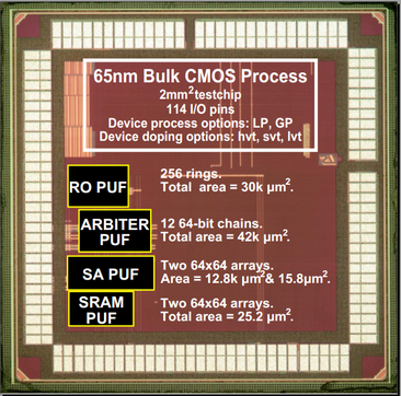
Generation I Testchip
The goal of this project is to design a secure and efficient PUF system. With a strong focus on circuit details, our research includes exploring the designs of the PUF core, the underlying circuit that generates the random bits, and is the source of all entropy in the PUF system. To that end, we have designed 2 testchips to provide us measurement data to support our analysis. The Generation I testchip (65nm bulk CMOS) was fabricated in November 2010 and contained test structures to provide an apples-to-apples comparison of security and VLSI metrics of various PUF types. It contained several other test structures (details below). Based on the measurement results, we then designed our Generation II testchip with improved test-structures and few novel designs and which was fabricated in June 2012 (details below).
Generation I Testchip:
On this testchip, we designed 2 delay based PUFs (arbiter and ring oscillator) and two bi-stable element based PUFs (SRAM and sense amplifiers). The details and results of this work can be found here (cicc'12).
In summary, we found that all PUF types can provide reasonably good randomness and uniqueness, however, all of them are poor in terms of reliability. Around 15-25% of PUF elements, for different PUF implementations, were found to be inconsistent when evaluated multiple times across +/- 20% VDD variations and a temperature variation of -20C to 85C, Applications that require high or perfect reliability need to implement ECC to correct these errors, but correction of such a high % of errors would result in an very high overheads of ECC, with may be prohibitive for many applications.
Further, we found that bi-stable PUFs have much better VLSI metrics (better area, power, and delay) compared to delay based PUFs for the generation of a raw response bit. We then explore if and how these superior VLSI metrics could be traded for higher reliability. Results for this analysis can be found here (cicc'12 and host'12).
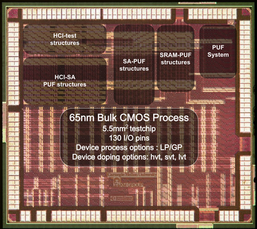
We then designed our Generation II testchip with improved test-structures and few novel designs to enable extreme enhancement of reliability in bi-stable PUFs. The chips are being tested now and the the results are to be published in conferences this year.
Generation II Testchip:
On this testchip, we designed various improved test-structures and few novel designs and which was fabricated in June 2012. The measurement results from this testchip are being collected now and not yet published.
Generation I Testchip:
On this testchip, we designed 2 delay based PUFs (arbiter and ring oscillator) and two bi-stable element based PUFs (SRAM and sense amplifiers). The details and results of this work can be found here (cicc'12).
In summary, we found that all PUF types can provide reasonably good randomness and uniqueness, however, all of them are poor in terms of reliability. Around 15-25% of PUF elements, for different PUF implementations, were found to be inconsistent when evaluated multiple times across +/- 20% VDD variations and a temperature variation of -20C to 85C, Applications that require high or perfect reliability need to implement ECC to correct these errors, but correction of such a high % of errors would result in an very high overheads of ECC, with may be prohibitive for many applications.
Further, we found that bi-stable PUFs have much better VLSI metrics (better area, power, and delay) compared to delay based PUFs for the generation of a raw response bit. We then explore if and how these superior VLSI metrics could be traded for higher reliability. Results for this analysis can be found here (cicc'12 and host'12).
We then designed our Generation II testchip with improved test-structures and few novel designs to enable extreme enhancement of reliability in bi-stable PUFs. The chips are being tested now and the the results are to be published in conferences this year.
Generation II Testchip:
On this testchip, we designed various improved test-structures and few novel designs and which was fabricated in June 2012. The measurement results from this testchip are being collected now and not yet published.
Generation II Testchip
|
<Details of the testchip will be provided after the results are published>
|
2. HIGH RELIABILITY SRAM USING PERIPHERAL LOGIC FAULT DETECTION AND ECC
Memory failures which occur after the manufacture-time burn-in testing phase are particularly difficult to address since redundancy allocation is no longer available and fault detection schemes currently used in industry generally focus on the data path while leaving the peripheral logic vulnerable to faults. Even in the data path, conventional error control coding (ECC) has been limited in its ability to detect and correct failures greater than a few bits. Using conventional ECC techniques to correct more than one bit per word incurs high latency, area, and power overheads.
For example, a typical implementation of random double bit error correction may require over ten cycles for correction and a large area for the encoding/decoding circuits and check bit and lookup table storage. Previously proposed low-overhead multi-bit soft error protection techniques perform poorly with randomly distributed hard errors because they assume either clustering error patterns or low error rates. Variability-induced hard errors are also a concern due to the high susceptibility of SRAM to variability effects due to the large number of near minimum-sized devices in the cell arrays. Consequently, conventional memory resilience techniques will be unable to counter the raw bit error rate of the
memory arrays in future technologies at economically feasible design points.
To address the effects of variability on the cell array, we have implemented on a 55nm bulk CMOS process a novel ECC scheme based on erasure coding that can extend conventional ECC already used in memory to correct and detect multiple erroneous bits with low latency, area, and power overheads. Our erasure-based ECC (EB-ECC) can correct two hard errors and detect one soft error per word without significantly increasing memory access latency. When EB-ECC is combined with an existing low-overhead soft error correction mechanism, our scheme can correct two hard errors and one soft error per word. The test chip containing this design was fabricated and is now back packaged and currently under testing.
